The Optics of Phase
Conventional lenses work by refraction: they redirect light by changing its propagation speed at a curved interface. A glass lens bends light because glass is denser than air, and Snell's law governs the deflection at each surface. This has worked beautifully since the seventeenth century — but it is not the only way to control light.
A diffractive optical element (DOE) works differently. Instead of bending light through bulk material, it imposes a precise spatial variation in phase across an incoming wavefront — manipulating light by controlling the path length each part of the wave travels. A flat surface etched with microscopic patterns can focus, split, shape, or scramble a beam with a precision and compactness that curved glass cannot match.
In two dimensions, DOEs are already ubiquitous: the holographic security patches on credit cards, the beam-shaping elements in laser projectors, and the flat metalenses that researchers are developing to replace bulky camera optics in mobile devices. But two-dimensional DOEs are only a fraction of what is physically possible. A truly three-dimensional diffractive structure — a periodic modulation of refractive index in all three spatial dimensions — can interact with light in qualitatively new ways.
This is the domain of photonic crystals and 3D diffractive elements, and it is an area where the manufacturing challenge is acute — and where self-assembly may offer a transformative solution.
Photonic Crystals: Controlling Light with Structure
A photonic crystal is a material with a periodic spatial modulation of refractive index, analogous to the periodic atomic potential in a crystalline solid. Just as atomic periodicity in a crystal creates electronic bandgaps — energy ranges where electrons cannot propagate — a photonic crystal creates photonic bandgaps: ranges of wavelength at which light cannot propagate through the structure, regardless of direction.
A material with a complete three-dimensional photonic bandgap would reflect light of the forbidden wavelength from every direction simultaneously. Photons in the bandgap range cannot exist inside the material. This has remarkable consequences:
A point defect (a missing lattice site) in a photonic crystal creates a localized electromagnetic mode — a cavity with, in principle, arbitrarily high quality factor. This is the ultimate optical resonator.
A line defect creates a waveguide that routes photons around sharp bends with zero radiation loss, regardless of bend angle.
An emitter placed inside a photonic crystal bandgap has its spontaneous emission completely suppressed (the Purcell effect), forcing it to emit only into engineered modes. This is the basis for thresholdless lasers and perfectly efficient single-photon sources.
But realizing a complete three-dimensional photonic bandgap requires a three-dimensional periodic structure with sufficient refractive index contrast, a favorable lattice geometry (face-centered cubic, diamond cubic, or gyroid are most suitable), and feature sizes comparable to the wavelength of light — on the order of 100–500 nm for visible wavelengths.
Fabricating such structures is extraordinarily difficult.
The State of the Art: Two-Photon Polymerization
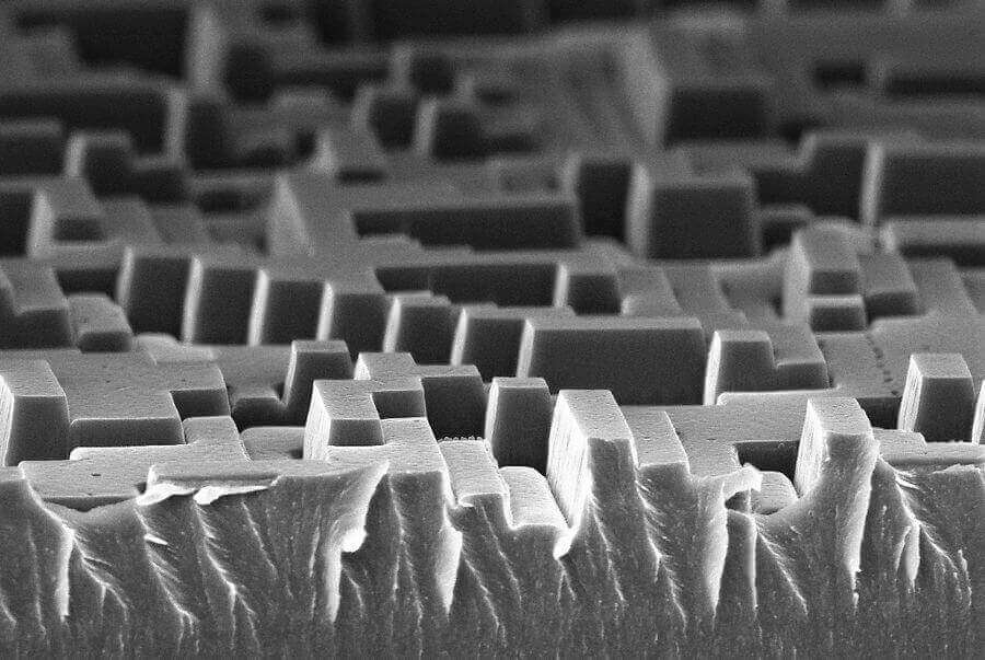
The gold standard for arbitrary 3D nanofabrication is two-photon polymerization (2PP), also called direct laser writing. A tightly focused femtosecond pulsed laser is scanned through a photosensitive resin, and at the focus, the peak intensity drives simultaneous two-photon absorption, triggering local polymerization. Because two-photon absorption scales as intensity squared, polymerization occurs only at the focal point — enabling voxels well below the diffraction limit, typically 100–200 nm lateral and 300–500 nm axially.
2PP has produced extraordinary demonstrations: photonic crystal templates, optical waveguides, mechanical metamaterials, microscale optical lenses, and entire microscale optical systems. Commercial 2PP systems (Nanoscribe, UpNano) write features at ~200 nm resolution with good fidelity.
But 2PP has a fundamental limitation: it is a serial process. Every voxel is written one at a time. A 100 × 100 × 100 μm³ structure at 200 nm voxel spacing contains approximately 125 billion voxels. Even at a voxel writing rate of one million per second, this volume takes over 34 hours to write. Scaling to macroscopic samples — even 1 mm³ — is entirely impractical.
Furthermore, 2PP produces amorphous polymer structures with relatively low refractive index contrast (~1.5), limiting the strength of optical effects. Achieving high index contrast requires post-processing — atomic layer deposition to infiltrate a high-index material, or pyrolysis to convert the polymer to silicon carbide — steps that introduce shrinkage and distortion.
A flat incoming wavefront enters the metalens from the left. The zone-plate pattern of TiO₂ (amber, high phase delay, n≈2.5) and SiO₂ (blue, low phase delay, n≈1.5) pillars imprints a spatially varying phase shift across the wavefront. The reshaped wavefront exits as a converging bowl that focuses to a diffraction-limited spot — the essence of flat-optic design.
Self-Assembly as a Competing Paradigm
Self-assembly offers a fundamentally different approach — one that is inherently parallel.
The key insight is that colloidal particles and block copolymers spontaneously assemble into periodic three-dimensional structures with unit cells in exactly the right size range for visible-light photonic crystals. The fabrication challenge shifts from "how do I write a billion voxels?" to "how do I program the right self-assembly geometry?"
Colloidal Crystal Fabrication
Colloidal crystal fabrication begins with monodisperse spheres — typically polystyrene or silica, with diameters from 100 nm to 1 μm — suspended in a liquid. When these spheres are allowed to sediment or are confined in a film, they assemble under the influence of electrostatic repulsion, van der Waals attraction, and capillary forces into face-centered cubic (FCC) or hexagonally close-packed crystals with long-range order over areas of square centimeters.
The colloidal crystal then serves as a template: a second material is infiltrated into the interstitial space (by sol-gel deposition, atomic layer deposition, or electrodeposition), and the original spheres are removed by calcination or solvent dissolution, leaving an inverse opal structure — a 3D periodic arrangement of spherical voids in a high-index matrix.
Inverse opals in silicon, titania (TiO₂), and other high-index materials exhibit photonic pseudogaps and, for sufficiently high index contrast (n > 2.8 for FCC), complete 3D photonic bandgaps. The fabrication, compared to 2PP, is strikingly simple: mix the colloids, let them assemble, infiltrate, calcinate.
The inverse-design loop: an adjoint gradient optimizer iterates over the 8×8 pillar array, toggling each pillar between TiO₂ and SiO₂ to minimize the error between the current output wavefront (orange) and the target focusing wavefront (green). Dipole-dipole coupling lines show interaction strength between adjacent mismatched pillars — they fade as the array converges to its optimal pattern.
Block Copolymer Self-Assembly: The Gyroid
While colloidal self-assembly produces FCC-based lattices, block copolymers offer access to a richer variety of three-dimensional periodic morphologies — including the gyroid, which has particularly favorable photonic bandgap properties.
Block copolymers phase-separate at the nanoscale to minimize unfavorable A-B contacts. The equilibrium morphology depends on the relative volume fraction of the blocks: spheres, cylinders, a bicontinuous gyroid network, or lamellae. The characteristic length scale is set by polymer chain length and is typically 5–100 nm.
The double gyroid morphology — two interpenetrating networks with cubic symmetry, connected by three-fold coordinated nodes — has a complete photonic bandgap when formed from materials with sufficient index contrast. Unlike FCC colloidal crystals (which require index contrast above ~2.8), the gyroid requires only ~1.5 — achievable with silicon or titania. Selective removal of one block leaves a nanoporous network that can be infiltrated with high-index material, retaining the gyroid topology with sub-20 nm feature sizes finer than what current 2PP can achieve.
DNA Origami for Precise 3D Optical Structures
For applications requiring precise, deterministic 3D structure (rather than the statistical perfection of a colloidal crystal), DNA origami offers an alternative self-assembly route with essentially atomic-level control.
DNA origami structures can be designed to carry optical components — fluorophores, gold nanoparticles, silver clusters — at specified positions with ~2 nm precision. DNA-mediated particle assembly has produced plasmonic dimers, trimers, and chiral clusters with designed optical chirality. Three-dimensional DNA origami cages carry gold nanoparticles at specific vertices of polyhedra, creating 3D plasmonic antennas.
More ambitiously, DNA-coated nanoparticles have been assembled into large three-dimensional colloidal crystals with designer lattice symmetries — including body-centered cubic, FCC, and simple cubic lattices with specific basis geometries — by programming Watson-Crick base-pairing interactions between particle-tethered DNA strands. The lattice constant can be tuned by adjusting the length of the DNA linkers, and the symmetry can be selected by using particles of two or more sizes with complementary DNA coatings.
This programmable DNA-mediated assembly provides access to lattice geometries not accessible to simple hard-sphere colloids, potentially including the diamond cubic lattice, which theoretically has the largest complete photonic bandgap of any known lattice geometry.
Head-to-Head Comparison
The two approaches occupy different regions of a multidimensional design space, and are ultimately complementary rather than competing:
Two-photon polymerization excels at arbitrary 3D geometry, precise defect placement, and integration with chip-scale devices — but is fundamentally serial, expensive, and limited in index contrast.
Self-assembly provides massive parallelism, scalability from nanoscale to macroscale, and access to high-refractive-index photonic crystals — but is constrained to periodic or quasi-periodic geometries and requires managing stacking faults and grain boundaries.
The logical synthesis: self-assembly provides the bulk periodic structure efficiently at scale, while a secondary 2PP or e-beam step defines macroscopic-scale features, waveguides, and input/output couplers. Hybrid approaches combining colloidal assembly with lithographically defined defects are already demonstrated in the literature.
Left: 2PP writes 200nm voxels one at a time — each cube lights up only after its write step. Right: 50nm SA particles converge simultaneously from random starting positions, finishing in a fraction of the time while delivering 4× finer resolution. The same target structure area is covered by 4× as many lattice sites in the SA panel, each carrying more optical detail.
The Path Forward: Challenges and Opportunities
Grain boundaries and disorder. Self-assembled structures inevitably contain grain boundaries, stacking faults, and point defects that scatter light. Improving long-range order — through surface templating, electric field alignment, flow-controlled deposition, and improved monodispersity — is an active research area.
Non-equilibrium assembly. All examples above rely on equilibrium self-assembly. Non-equilibrium approaches, where energy input (light, oscillating fields, chemical reactions) maintains the system in a dynamic steady state, can produce structures inaccessible to equilibrium thermodynamics. Active matter and driven colloidal systems are beginning to show how this might be achieved.
Functional incorporation. Photonic crystals become truly powerful when embedded with gain media, nonlinear optical materials, or active components. Incorporating these materials during self-assembly — rather than after — is a challenging but tractable problem. Quantum dots, rare-earth emitters, and two-dimensional materials (MoS₂, hexagonal boron nitride) are being integrated into colloidal crystal hosts.
Integration with chip-scale photonics. The eventual application of 3D self-assembled photonic structures requires integration with waveguides, detectors, and light sources on chip substrates. Directed self-assembly in lithographically defined templates is a promising route: the lithography provides coarse spatial registration; the self-assembly provides nanoscale feature definition.
Self-assembly will not replace two-photon lithography for applications requiring arbitrary 3D geometry. But for the large class of applications requiring three-dimensional periodic structures at optical scales, self-assembly offers a path to scalable, affordable fabrication that would be entirely impractical to write one voxel at a time. As the techniques for controlling self-assembly geometry, incorporating functional materials, and managing defects mature, this approach may prove to be the practical route to 3D photonic integration that the field has long sought.
The ribosome, after all, assembled itself.